6.24.2012

与其担心未来,不如现在好好努力


当你在犹豫的时候,这个世界就很大;当你勇敢踏出第一步的时候,这个世界就很小。等到有一天你变成了你喜欢的自己的时候,谁还会质疑你的选择不靠谱呢?你已经变成更好的你了,一定会遇到更好的人的。你是谁,就会遇到谁。
 
1. 其实在这个世界上没有一份感情不是千疮百孔的。
 
我有个朋友A,他恋爱谈了7年还是分手了。那阵子他看起来跟个没事人一样,我们都以为他没那么在意,结果有一天他喝醉了,莫明地哭了很久。第二天他醒过来,对我说了一句特文艺的话:“其实在这个世界上没有一份感情不是千疮百孔的。”
 
行走世间,全是妖怪。
 
记得之前人人上这篇日志很红,里面的内容我已忘记了大半,却对这句话记忆深刻。后来我在文里写,青春的另外一个名字叫做徒劳。这样的一种徒劳无功,在于你无论怎么过,过的是挥霍是珍惜,等到以后你回想起来,都会觉得不够好。就像你很喜欢一个人,却明明知道你们不可能走到最后,最可怕的就是你明明知道这一点,却没办法改变它。
 
曾经我和我妈讨论过这个问题,她说明明不可能在一起还要谈恋爱,这样就是一种不靠谱。我说,没关系,现在我哪怕跌倒了也还能爬起来。
 
2. 选择一个你喜欢的,还是一个喜欢你的。
 
朋友B今天突然跟我聊起天来,她问我“你将来是会选择一个你喜欢的,还是一个喜欢你的。”我想了很久始终不知道应该怎么回答她,我本以为按照我的个性,一定会说选择一个我喜欢的,再加上一句“我从不怕爱错,只怕没爱过”之类的文艺的话。
 
却没想到我踌躇了。
 
选择一个我喜欢的怕受伤,怕不靠谱;选择一个喜欢我的很安稳,却又怕自己不甘心。
 
她说年龄已经摆在那里了,拖不起了,还是选择一个喜欢自己的,也许会比较幸福一点。她说:以前对她来说,梦想比什么都重要,一心就想读研,现在却什么都不想了,只想早点回家,一点也不想累,不想做个女强人,想随便找份稳定的工作稳定的老公稳定的家庭,就这么算了。
 
3.昂首挺胸走过的人生是唯一的骄傲。
 
出书以后我就常常接到各方面的留言,问题不外乎怎么摆脱寂寞,怎么看待未来,怎么看待梦想。往往我都不知道怎么回答他们,直到元旦那天,凌晨4点的我还在赶稿子,合上电脑的我睡眼惺忪却突然明白了:那些喜欢你的总有一天会不喜欢你,那些你抓紧的总有一天会抓不住,那些你想实现的梦想也许根本实现不了,那些曾经以为无比重要的总有一天会变成不重要的。
 
不过这些其实都没什么,很多年以后你回想起来,唯一让你觉得真实,和骄傲的,是你昂首挺胸用力走过的人生。
 
我也许从来就摆脱不了所谓的寂寞,也看不清所谓的未来,也道不明为什么要这么努力去实现梦想,可是我依旧在做。好比如果在剧场开始的时候就告诉你和她的结局,你会说没关系我知道啊我还是爱你,还是会转身离去。如果是我,我一定还会去喜欢她,仅此而已。
 
我宁愿让别人觉得我是变形金刚百毒不侵面面俱到不知疲倦,我也不要让别人看到我难过疲倦跌倒失落。我不喜欢去抱怨,因为我知道没人喜欢听抱怨。
 
4.做自己喜欢的事情也是一种回报。
 
其实爸妈一直觉得我挺不靠谱的,连我自己都这么觉得。我是那种对你百般好感未必说,对你千般厌恶未必讲的人,宁可自己内伤憋得严重,也要假装不在乎你,宁可在你消失的时候比谁都着急满世界找你,也要在你出现的时候假装不经意。
 
老妈至今还一口玩笑的语气说我:“你看看你,谈不靠谱的恋爱,写没人看的书,去没人知道的地方,真是不靠谱。”他们总觉得我现在这样太辛苦,每天日夜颠倒,想把我弄到家附近的单位工作。其实我不是没想过,回来离家又近又方便而且赚的也不会少,可是我还是拒绝了。没错,也许写书是挺不靠谱的,但是我觉得没什么。写作就是写作的回报,画画就是画画的回报,唱歌就是唱歌的回报。如果人真的能做自己喜欢的事情,谁说这不是一种回报呢。
 
有时间我就每天花两小时看书,没时间就睡前看二十分钟,周末的话可以看完整本书。做论题做一遍做不好我就做两遍,文稿要求我写一万字我就写将近两万字然后删。写出一篇好文是运气,如果一个人一直在写的话,那就是靠努力。更多时候,世界对你的态度取决于你对世界的态度,没什么好抱怨的。
 
其实这都没什么,有个朋友每天晚上8点必须看部电影然后喝点红酒伪小清新然后11点准时睡觉,住在楼上的小伙天天早上5点就起床跑步,而我那个时候往往还没睡。
 
我们都会找到属于自己的生活节奏,然后沉溺其中无法自拔。
 
5. 不靠谱和安稳归根结底是安全感的问题。
 
我不知道是不是还有很多人面临着像我这样子的选择。其实大多数时候,不管我们选择不靠谱还是很安稳,我们都面临着一个很重要的问题。这个问题归根结底是三个字:“安全感。”
 
后来我才想明白了,与其担心未来,不如现在好好努力。这条路上,只有奋斗才能给你安全感。不要轻易把梦想寄托在某个人身上,也不要太在乎身旁的耳语,因为未来是你自己的,只有你自己能给自己最大的安全感。别忘了答应自己要做的事情,别忘了自己想去的地方,不管哪有多难,有多远,有多“不靠谱”。
 
当你在犹豫的时候,这个世界就很大;当你勇敢踏出第一步的时候,这个世界就很小。等到有一天你变成了你喜欢的自己的时候,谁还会质疑你的选择不靠谱呢?你已经变成更好的你了,一定会遇到更好的人的。你是谁,就会遇到谁。
 
重要的是,不管是做怎么样的选择,都要对得起自己的内心。就像上面写的一样:很多年以当你在此回想起来,唯一让你觉得真实,和骄傲的,是你昂首挺胸用力走过的人生。

6.23.2012

小心成功毁了我们的人生

前不久老友小聚,遇到了N年未曾谋面的朋友A,若干年前干瘦如柴的他,如今已经发福得厉害,直逼那些低头看不到脚面的孕妇。衣着也光鲜,端的是有了身家的姿态。仔细一打听,原来已经在小城里荣升为某科局的领导。

因为对坐的是我们一班头上没有乌纱帽的人,所以A自然迅速确认了自己的首领地位,一餐饭之间,别人只能当听众,听他说些官场是非,不是谁升了正处,就是谁有了豪宅,再有就是反复提及的当年勇,说的是一个草根如何闪展腾挪使出十八般武艺爬上现在位子的得意。至于我们这些当年一个战壕里摸爬滚打过的无名小卒——本人来吃这顿饭,分明是给你们赏光了。

我没有那么狭隘的肚肠,听不得别人的得意,只是,仰望一个人得意到忘形的表演,还是很有点感慨的。当年的A本性敦厚,忠厚善良,从不乱打诳语。却不想,只是短短几年,竟然沦落到了如此市侩的嘴脸,不能不叫人感喟成功二字毁人的力量。

连带着想起故乡村子里的一个支部书记。原来也是本分的庄稼人,后来同乡里的干部扯上关系,当上了一村之长。人人都说他变了样子,初始我还不信,不久因为父母要在村里盖房子,于是提了两瓶酒去拜见。因我还算有个公职人员的身份,所以他比对别人要客气几分。只是,那寒暄,先是问候了我们局长,亲热得像是拜了把子的兄弟,又提到了县长,却随随便便地大手一挥:那些鸟人,都水平一般了。

我听得眼珠子都要掉出来。好歹听他咋呼完了告辞出来,想到一个问题:一个人如果极度自我膨胀到一定程度,会像气球一样爆裂吗?

没过两三年,老家父兄传来消息,那位牛气冲天的村支书,因为贪污了几万元的公款,锒铛入狱了!

自恋是人类的通病,大多平常人因为尚有自视的功力,所以大部分时间还算能把握得住。可总有些人,在追逐世俗定义的“成功”时,渐渐失去了人类本身的纯良。

前段时间,李阳家暴的事情在网上炒得沸沸扬扬,我凑热闹跟着去看,就看到了柴静对李阳的访谈。

让我震惊的是李阳那副淡然冷漠的样子。说到三个孩子,他凛然看着镜头,大言不惭:亲情是一种丑陋的东西;又提到老婆,还是一如的淡然:对我来说,婚姻只是场实验;再提到自己的父亲,李阳用了另外一个词语——恶心。

我震惊到无以复加的地步。之前,只知道李阳是成功的斗士,却不想,在巨大的斗士光环背后,竟然深藏着这样冷酷无情的灵魂。

柴静问得很无力:“那你活着的终极目标是什么?”

“成功”。李阳简洁地回答了这两个字,那一刻,他的眉宇间,跳动的是异样的光彩和喜悦。

为了成功,为了夺取众人的眼球和注视,这个男人,上飞机的时候总是最迟到的那一个。要的就是,空姐通过喇叭喊他上机的那种感觉,要的就是在一机舱的人注视下款款而来的风度。为了要这种注视,他甚至不在乎别人的目光中,是不是有厌弃和鄙视。

睿智的柴静面对李阳,也终是哑口无言了。作为观众,我感到的是同样深刻的悲凉。成功膨胀了他的野心,也膨胀了他的自我定位,一个李阳毁灭在成功的起点上,更多的李阳,同样前赴后继地在成功脚下折戟沉沙。

所以,请一定小心,小心“成功”打着华丽的幌子,就那样润物无声地腐蚀和掠夺了你我的人生。

傻逼一样坚持,总会看见牛逼的结果

如果一件事成功率是1%,那反复100次至少成功1次概率是多少?备选答案:10%,23%,38%,63%——正确答案是63%。计算方法: 成功率1%,失败率99%,尝试100次,全部失败概率为99%的100次方约37%,至少成功一次即63%。看似不可能的事在反复尝试中成功率会不断提高——傻逼一样坚持,总会看见牛逼的结果。

这是今天同事在RTX群里分享的每日一则,咋看之下,觉得没什么问题。因为单单从数学概率角度去计算,上面问题的答案是完全正确。但考虑到实际的操作过程会存在一些干扰因素,可能会影响到每一次尝试的成功率,我们可以深层次的讨论。


1、如果这件事情存在完全不可操控因素,即:这件事情尝试了一次或者多次,即便都失败了,所获取的经验并不能让你在下一次尝试过程中减少一些失败的可能。那么上述问题中的思路和答案都是正确的。但是结论的表达是有一些问题:因为事件本身的单次成功率是没有提高的,还是1%。所以,这个结论前半句并不可取。如果有人能把所有的错误尝试一遍之后,对于当事人而言,下一次的尝试自然是成功。所以后半句倒是可取:傻逼一样坚持,总会看见牛逼的结果。


2、现在考虑第二种假设,如果这件事情是一件固定的事务,不存在随机改变的因素。可以看做是在做一道有100个选项的选择题,那么每失败一次,下一次仍然失败的概率就会减少一些。如果对自己每一次的失败都做记录,那么最糟糕的情况是,前面99次每一次都选错了,那么最后一次必然是会正确的。其实这个 过程中,每一次失败之后的下一次选择的正确率也在提高,从第一次开始分别是:1/100,1/99,1/98… 这样的话,反复去重复100次,至少成功一次的概率就是100%。最糟糕的情况就是第100次的时候成功了。

这种情况下,第n次仍然失败的概率是:

(99/100)(98/99)*…*(101-n+/102-n)*(100-n/101-n)
=(100-n)/100

可以看出,随着n的增加,也就是尝试次数的增加,失败的概率会越来越小。直到第一百次失败的概率减小为0。

这种情况,完全可以得到上述结论:看似不可能的事在反复尝试中成功率会不断提高——傻逼一样坚持,总会看见牛逼的结果。


3、另外一种情况,也是现实生活最常见的情况。

如果这件事情是存在一些不可控因素,但并不是完全无规律可循。比如创业,或者远距离的投篮。不同的人在失败的过程中所获取的信息是不同的,多数人而言,每一次尝试,如果没成功,也可以获知到对成功存在障碍的因素,下一次尝试的时候,尽量避免在同一个地方跌倒,哪怕是换一个地方跌倒。

这个概率是无法用具体的数字来度量,但是显然,在我们每个人身边,我们可以看到,几乎所有人都会有一两个比较擅长的领域,还有些人是解决问题的高 手,总是很容易成功。因为我们生活中遇到的问题往往并不是完全随机。很多事情,比如投篮命中率,比如限时回答问题,通过不断地练习,更好的掌握力度,方向,弧度等技巧,这个不断练习,不断尝试的过程中无疑是提高了单次尝试的成功率。 同样,一个人在一个领域有一定经验之后,换一个领域也会比较容易成功。因为问题多半会有相通的部分,掌握了学习的能力和解决问题的能力,即便在不同的领域也一样。

同时,即便是同一件事情,不同人的表现是不一样的。在失败的过程中,有些人自信心受到打击,选择放弃,下一次如果不得不去做这件事情的时候,反而有了阴影,克服不了自己的障碍,成功率反而会更低。另外一部分人,越挫越勇并且善于总结失败的教训、分析事情之间的关联,那么这些人做事的成功率无疑是会越来越高的。

看似不可能的事在反复尝试中成功率会不断提高——傻逼一样坚持,总会看见牛逼的结果。 这种情况是很容易得出这个结论的。


4、但上面三种情况并不能足以证明“傻逼一样坚持,总会看见牛逼的结果”这一个结论,因为还存在一个问题。

反复做一件事的问题中的前提条件是:看似不可能的事件。这种事件可以分为两种的:小概率事件和不可能事件。上面三种情况分析的都是小概率事件。对于后者——不可能事件,反复尝试的结果是徒劳的。虽然都是傻逼一样的坚持,但是有些人最后牛逼了,有些人傻逼了。所以,在这个过程中,如何判断一件事情是小 概率事件还是不可能事件,就很重要。

爱因斯坦说:疯狂就是重复做一件事,但期待不同的结果。

所以有些人疯狂之后成功了,有些人就真的疯了。个中缘由,见仁见智吧。

6.20.2012

不要让需要你的人觉得你太好,而是要让他觉得这个世界很美好

这桩谋杀案很奇特,死者是出了名的好好先生,小镇的人甚至评价他,这辈子都没跟人斗过嘴。

没有仇人,没有妻儿子女,每天本本分分地在不远的一所私立学校教书,按时上下班,周末去做礼拜,虽然不是有太多人喜欢他,但也从来没有人讨厌他。

没有病史,更不是意外,谁会对这样一个人下狠手,竟然一刀直插进胸膛,毫不留情的手法。

警察调查了小镇所有录像,全是熟人,有一两个陌生人也能提供充分的不在场证据,所以,这是一桩棘手的谋杀案。


电视台天天在报道,小镇居民惶恐不安,警察局压力很大,只好整天跑到死亡现场取证,寻找线索,可惜,这一切都是徒劳。

这个案子一直悬了三十年,而且,三十年后也并不是警方成功破案,而是凶手无意间泄露了天机,我要讲的重点便在这里。

那是在伊顿公学的开学典礼上,学校请来了着名的商业大家艾维尔先生作励志演讲,他一生坎坷,从一名乞丐奋斗到如今的成就,很多媒体都报道过他的事迹。

可他为什么会被警察盯上,只因为伊顿公学的一位学生提了一个问题,艾维尔先生,你那么富有,可为什么不做慈善呢?

事实也的确如此,连伦敦电视台着名主持人马森都曾公开调侃过,说艾维尔先生真像莎士比亚戏剧里的一个男主角,是谁呢?夏洛克。

哦,对不起,回到伊顿公学的问题上。当时,艾维尔先生迟疑了片刻,接着便说出了惊世骇俗的一段话:“如果我去做慈善,那么,我会杀死很多人,或者,我被很多人所杀。”

这是什么意思?没有人能理解艾维尔到底在讲什么,最后还是一旁的主持人打了圆场:“艾维尔先生,您能给我们的孩子们讲得更具体一点吗?”

“当然!”艾维尔的演讲出现在电视屏幕上,他非常自信地站在演讲台上说:“我认为,一个人的成功来自于他的不满足,只有不满足于现状,面临着生存压力,他才会最大限度地发挥自身的能量,去争取自己的生存空间,实现自身的价值,因为不满足,所以我才有今天。”

全场立刻响起热烈的掌声,确实,艾维尔先生用一生的奋斗证明了他的价值,可是,这与慈善有什么关系?所以,主持人趁着全场热烈的气氛,立马追问,既然如此,为什么不做一点慈善去帮助那些难以生存的人呢?

“你错了,如果我是一个没有生存空间的人,我就不希望任何人施舍我,因为别人的慈善会让我觉得满足,觉得不争取也能活下去,谁这样对我,就是在害我,我宁愿把身边这样的好人杀死。”

就是因为这段话太过震撼,虽然其中不乏真谛,但当电视台热播出来时,一位当年的老警察觉察出了一丝端倪,艾维尔曾经就是一位乞丐,二十年前,他就在那起谋杀案现场附近乞讨,只不过,谁都没想到他会是凶手。

谋杀案告破之后,报纸上一行叙述触目惊心:“他每天都会给我一点钱,我讨厌他这样子对我,如果他不死,我就永远站不起来,他要杀死我的希望,我就要杀死他。”

这是发生在英国温莎小镇的一桩真实谋杀案,因为这桩谋杀案,当地居民特意在小镇立了一块“自省碑”,上面是当地一位着名绅士亲手刻的碑文:不要让需要你的人觉得你太好,而是要让他觉得这个世界很美好。

6.09.2012

How to Make a CPU: From Sand to Shelf

Enter Sand, Man

We’re pretty sure that most computer enthusiasts are aware that CPUs are made from silicon. Far fewer are likely to realize exactly how much work goes into making what is effectively a wonder of the modern world. Processors are made on a mind bogglingly small scale to withstand huge tolerances, with even the cheapest chips requiring hundreds of manufacturing stages to get from wafer to motherboard.

Manufacturers are also under pressure to improve production methods and reduce transistor size, with different companies approaching the problem in different ways. Intel helped us put this guide together, and as a result it focuses on its implementation of the 32nm High-K manufacturing process. Other manufacturers, such as Global Foundries or TSMC, use subtly different methods to produce its chips. 


Left: Its got a long way to go from here. Right: It's important to make the silicon ingot a single, join-less piece.

Amazingly, after oxygen, silicon is the most plentiful element in the earth’s crust. It’s not just lying around in electronics-grade lumps though, and needs to be extracted from sand, where it resides in the form of silicon dioxide (SiO2). 

Once the silicon has been purified to the required degree (something in the region of 99.9999999 per cent pure), it's formed into a single contiguous 100kg ingot of silicon. The ingot can then be sliced into individual 1mm thick disks, called wafers, which should be recognizable to most tech junkies.

  
Left: These ingots weigh up to 100kg and are around 12 inches in diameter. Right: The wafers have to be precisely the right thickness.

The wafers are then polished to a flawless mirror finish ready for the next stage of the process. Interestingly, CPU manufacturers are not normally responsible for these initial stages, instead buying ready cut and polished wafers from third-party silicon producers.

 
Left: The cut and polished silicon wafer all ready to be made into a few hundred processors. Right: You can just see the patterned sheen of the photo resist.

Now the complex business of creating something capable of playing Crysis and rendering video begins in earnest. The wafer is covered in a strategically pattered layer of photo resist, which acts like a stencil for when the wafer is bombarded with high powered beams of charged atoms called ions. 

  
Left: Beam me up Scotty... or just embed me with trillions of charged ions. Right: The electrical conductivity of certain parts of the wafer has now been changed.

The ions embed themselves in the exposed parts of the silicon, in a process called ion implantation or doping, leading to a change in the conductive properties of that part of the wafer. The photo resist is then removed, leaving behind a complex pattern of conductive and non conductive traces on the silicon wafer.


Special K

The next stage is to add the High-K dielectric material, which performs the same role as the traditional silicon-dioxide insulator. It’s actually this specialized High-K material that has helped Intel to implement the transition from 65nm to 45nm and now to 32nm production processes, as it's superior to traditional insulators in a number of ways that will be highlighted later.

If we were focusing on the production of a chip made on a less advanced production process, then a more traditional silicon-dioxide material would be used at this point.

 
Left: The yellow sheets represent layers of High-K dielectric... obviously. Right: The dielectric is added in layers only one atom thick to give a perfect finish.

The dielectric is added in microscopic layers, literally only an atom thick at a time. Adding the dielectric in this manner allows greater accuracy and reduces potential electrical leakage, leading to more energy efficient processors in the long run.

The High-K material is also applied in a thicker layer than with traditional insulators, but still retains the same capacitive properties as these materials. This allows electrical leakage to be reduced (due to the thicker material) without affecting capacitive performance, a property which is key to making manufacturing at these tiny sizes possible.


Left: The wafer is spun to distribute the photo resist evenly. Right: The masks used in the photo lithography are incredibly detailed.

Another layer of photo resist is then added. The wafer is then exposed to a specific pattern of ultra violet light which turns sections of the photo resist soluble, in a process called photo lithography.

The pattern of light is achieved by using finely detailed ‘masks’, which act like stencils. These masks, detailed as they are, still need to be focused down to the microscopic levels that current CPUs work at. This is done by passing the masked light through a lens, which typically reduces the size of the mask's image by four times.


Left: We've zoomed down to look at a single transistor now. The dark line in the centre shows where the mask stopped the UV light reacting with the photo resist. Right: The UV-reacted photo resist is removed with gentle solvents.

The photo resist exposed to the light can now be removed with a solvent, leaving behind a specific pattern of unaffected photo resist created by the mask. This photo resist then protects the pattern of High-K dielectric it still covers, while the excess High-K material is gently etched away using chemicals.

 
Left: The photo resist also resists the etching chemicals. Right: The yellow strip is the High-K dielectric, and the green is the doped conductive silicon.

The photo resist is then removed leaving an incredibly intricate pattern of High-K dielectric on top of the conductive and non conductive silicon.


Interconnected

The wafer is then covered in a layer of insulation material. At this stage the transistors are actually complete, but they are completely isolated from each other. To make a functioning chip the transistors need to be able to talk to their hundreds of millions of siblings, and the next stage in the process - metal deposition - allows this.

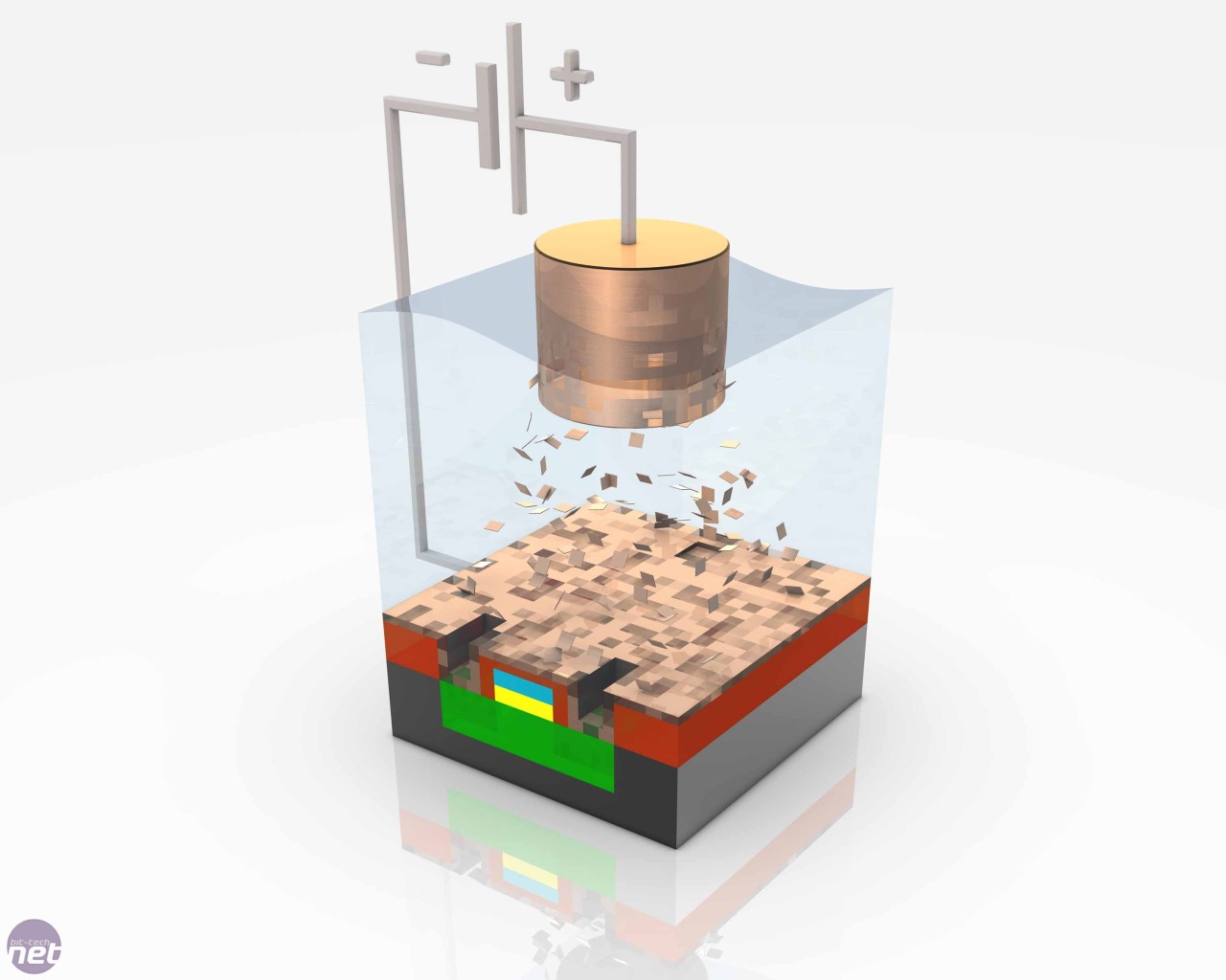
Initially three holes are etched at strategic points in the insulation layer above each transistor. The entire wafer is then placed into a copper sulphate solution and electroplated. 
  
Left: The red layer is the newly added insulator, note the three tiny holes. Right: Electroplating, just like in GCSE chemistry

Electroplating a CPU wafer is exactly the same process many people will have either tried or seen done at school in chemistry class, and involves placing a negatively charged object (the cathode) into a metal salt solution. The metal salt contains positively charged ions which are attracted to the cathode (in this case, the wafer) and ‘reduce’ themselves upon the cathode to form an even metal layer over the object.

This leaves the entire wafer covered in a thin sheen of pure copper which now needs to be removed. This is done through a delicate polishing process which polishes the wafer back to the insulation layer, leaving copper still deposited in the three holes etched earlier in the process. 

  
Left: Electroplating gives a perfectly smooth finish. Right: The transistor polished back to the insulator. Note the three holes are now filled with copper.

The transistors are now primed with metal contacts and just need wiring up; unfortunately wiring up hundreds of millions of microscopic transistors is a mind-bendingly complex task. It is also incredibly important, as this is where the performance crown can be won or lost - the stages up to this point are standard processes for making ICs and transistors.

It is the intricacies and complexities of the transistor interconnects of the chip that will eventually dictate individual performance and efficiency, so getting this stage correct is of paramount importance.


Left: This shows the interconnects between just six transistors - intricate is an understatement. Right: Basic quality control is also conducted at this point

The interconnects are built up in levels with modern chips, with up to 30 levels of interconnects arranged above the surface of the chip in a bewilderingly complex fashion. Indeed, if you were so inclined, you could lever off the heatspreader on your CPU and take a look at the chip under a microscope. Having done this you would see what looks like a flat and smooth chip is in fact a complex 3d object, with Intel describing the intricate network of circuit interconnects as 'looking like a futuristic, multi-layered highway'.


CPUs Got Talent

At this point the processors are complete and all that is left is to test, package and speed bin the chips. Testing is conducted at a basic level while the dies are still in wafer form, with a simple test algorithm given to the chip. Any chips outputting the wrong answer are marked and discarded once the wafer has been delicately cut into individual CPU dies. 


Left: We're almost sure they don't use circular saws for this... Right: The completed and cut die - in this case a Clarkfield CPU and GPU destined for a Core i5

Individual dies are then ready to be packaged into what many people would recognize as a CPU. The die sits on a substrate (or PCB) in a socket that connects it to the pins or contact points of the packaging. The chip is then glued in place, and a heat spreader placed on top of it to help effectively conduct heat away from the chip.

  
Left: A delicate socket on the substrate of the CPU package connects the die to the pins or pads on the underside. Right: Speed binning - the X-Factor of the CPU world.

Once the chips have been packaged they go through a class testing or ‘binning’ process whereby their thermal and frequency characteristics will be analysed. Think of it as an audition process, with each chip hoping to be capable of getting a role at the top end of the range, running at the highest frequencies. Unfortunately, due to tiny variances in the production process, some chips may not run as well and will have to be content with being binned as lower range chips - at least they avoid a cringey interview with Ant and Dec.

Once the chips are binned and packaged they can be send out to system builders in trays of 1,000, or to online retailers in their more flashy retail packaging, ready to be bought and put through their paces by the public. 


Left: CPUs get sent to system builders in trays. Right: Consumers get the fancy packaging.

The lucky CPUs may end up spending their life rendering the beautiful landscapes of the latest games and videos, or even help create the next CGI Blockbuster. However, spare a thought for the poor, tortured chips that spend their life sweating and straining in one of James’s myriad of folding rigs.