We’re pretty sure that most computer enthusiasts are aware that CPUs are made from silicon. Far fewer are likely to realize exactly how much work goes into making what is effectively a wonder of the modern world. Processors are made on a mind bogglingly small scale to withstand huge tolerances, with even the cheapest chips requiring hundreds of manufacturing stages to get from wafer to motherboard.
Manufacturers are also under pressure to improve production methods and reduce transistor size, with different companies approaching the problem in different ways. Intel helped us put this guide together, and as a result it focuses on its implementation of the 32nm High-K manufacturing process. Other manufacturers, such as Global Foundries or TSMC, use subtly different methods to produce its chips.


Left: Its got a long way to go from here. Right: It's important to make the silicon ingot a single, join-less piece.
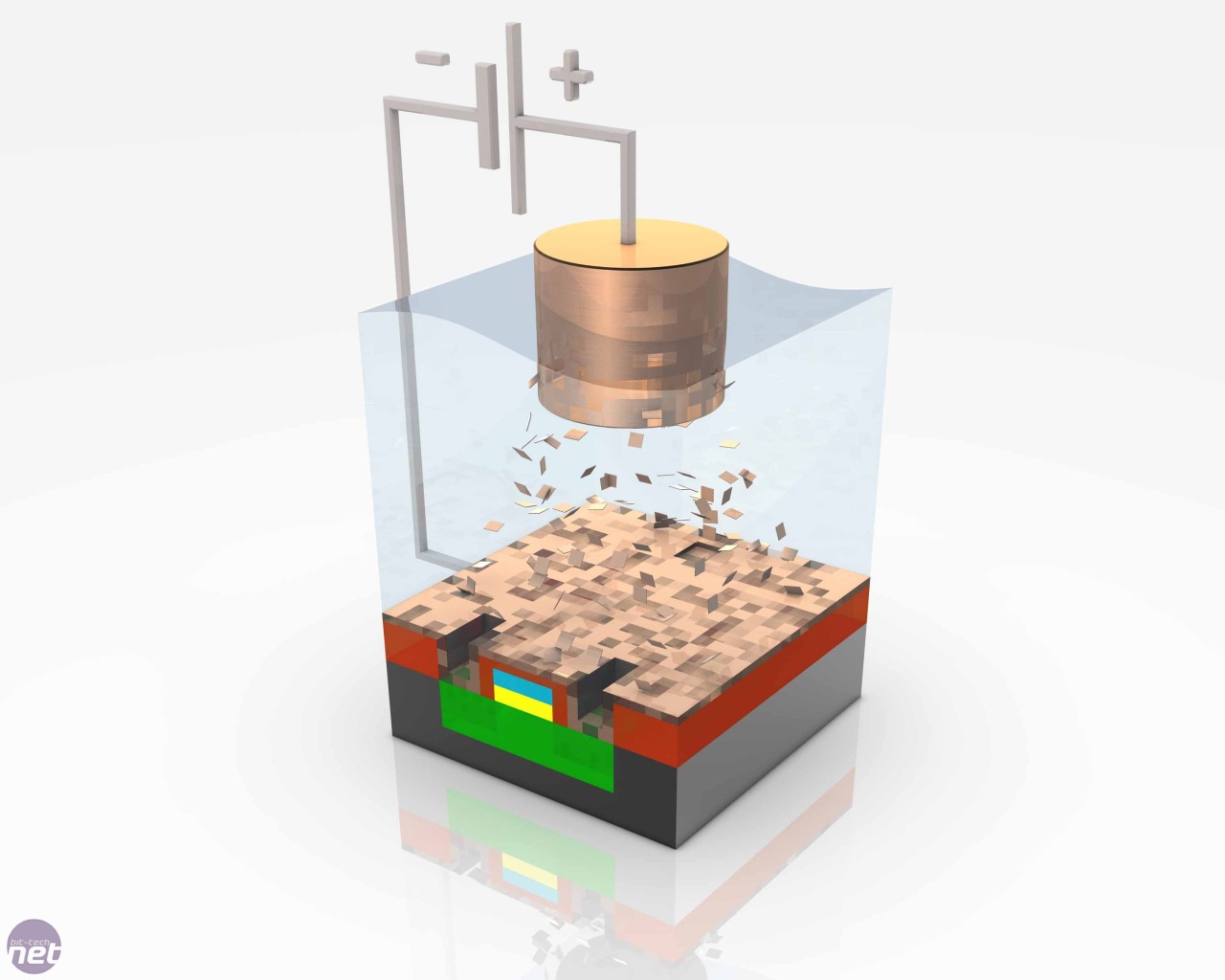
Amazingly, after oxygen, silicon is the most plentiful element in the earth’s crust. It’s not just lying around in electronics-grade lumps though, and needs to be extracted from sand, where it resides in the form of silicon dioxide (SiO2).


Left: These ingots weigh up to 100kg and are around 12 inches in diameter. Right: The wafers have to be precisely the right thickness.
The wafers are then polished to a flawless mirror finish ready for the next stage of the process. Interestingly, CPU manufacturers are not normally responsible for these initial stages, instead buying ready cut and polished wafers from third-party silicon producers.


Left: The cut and polished silicon wafer all ready to be made into a few hundred processors. Right: You can just see the patterned sheen of the photo resist.
Now the complex business of creating something capable of playing Crysis and rendering video begins in earnest. The wafer is covered in a strategically pattered layer of photo resist, which acts like a stencil for when the wafer is bombarded with high powered beams of charged atoms called ions.


Left: Beam me up Scotty... or just embed me with trillions of charged ions. Right: The electrical conductivity of certain parts of the wafer has now been changed.
The ions embed themselves in the exposed parts of the silicon, in a process called ion implantation or doping, leading to a change in the conductive properties of that part of the wafer. The photo resist is then removed, leaving behind a complex pattern of conductive and non conductive traces on the silicon wafer.
Special K
The next stage is to add the High-K dielectric material, which performs the same role as the traditional silicon-dioxide insulator. It’s actually this specialized High-K material that has helped Intel to implement the transition from 65nm to 45nm and now to 32nm production processes, as it's superior to traditional insulators in a number of ways that will be highlighted later.
If we were focusing on the production of a chip made on a less advanced production process, then a more traditional silicon-dioxide material would be used at this point.
If we were focusing on the production of a chip made on a less advanced production process, then a more traditional silicon-dioxide material would be used at this point.


The dielectric is added in microscopic layers, literally only an atom thick at a time. Adding the dielectric in this manner allows greater accuracy and reduces potential electrical leakage, leading to more energy efficient processors in the long run.
The High-K material is also applied in a thicker layer than with traditional insulators, but still retains the same capacitive properties as these materials. This allows electrical leakage to be reduced (due to the thicker material) without affecting capacitive performance, a property which is key to making manufacturing at these tiny sizes possible.


Another layer of photo resist is then added. The wafer is then exposed to a specific pattern of ultra violet light which turns sections of the photo resist soluble, in a process called photo lithography.
The pattern of light is achieved by using finely detailed ‘masks’, which act like stencils. These masks, detailed as they are, still need to be focused down to the microscopic levels that current CPUs work at. This is done by passing the masked light through a lens, which typically reduces the size of the mask's image by four times.


The photo resist exposed to the light can now be removed with a solvent, leaving behind a specific pattern of unaffected photo resist created by the mask. This photo resist then protects the pattern of High-K dielectric it still covers, while the excess High-K material is gently etched away using chemicals.


Left: The photo resist also resists the etching chemicals. Right: The yellow strip is the High-K dielectric, and the green is the doped conductive silicon.
The photo resist is then removed leaving an incredibly intricate pattern of High-K dielectric on top of the conductive and non conductive silicon.
Interconnected
The wafer is then covered in a layer of insulation material. At this stage the transistors are actually complete, but they are completely isolated from each other. To make a functioning chip the transistors need to be able to talk to their hundreds of millions of siblings, and the next stage in the process - metal deposition - allows this.
Initially three holes are etched at strategic points in the insulation layer above each transistor. The entire wafer is then placed into a copper sulphate solution and electroplated.

Left: The red layer is the newly added insulator, note the three tiny holes. Right: Electroplating, just like in GCSE chemistry
This leaves the entire wafer covered in a thin sheen of pure copper which now needs to be removed. This is done through a delicate polishing process which polishes the wafer back to the insulation layer, leaving copper still deposited in the three holes etched earlier in the process.


Left: Electroplating gives a perfectly smooth finish. Right: The transistor polished back to the insulator. Note the three holes are now filled with copper.
The transistors are now primed with metal contacts and just need wiring up; unfortunately wiring up hundreds of millions of microscopic transistors is a mind-bendingly complex task. It is also incredibly important, as this is where the performance crown can be won or lost - the stages up to this point are standard processes for making ICs and transistors.
It is the intricacies and complexities of the transistor interconnects of the chip that will eventually dictate individual performance and efficiency, so getting this stage correct is of paramount importance.


Left: This shows the interconnects between just six transistors - intricate is an understatement. Right: Basic quality control is also conducted at this point
The interconnects are built up in levels with modern chips, with up to 30 levels of interconnects arranged above the surface of the chip in a bewilderingly complex fashion. Indeed, if you were so inclined, you could lever off the heatspreader on your CPU and take a look at the chip under a microscope. Having done this you would see what looks like a flat and smooth chip is in fact a complex 3d object, with Intel describing the intricate network of circuit interconnects as 'looking like a futuristic, multi-layered highway'.
CPUs Got Talent
At this point the processors are complete and all that is left is to test, package and speed bin the chips. Testing is conducted at a basic level while the dies are still in wafer form, with a simple test algorithm given to the chip. Any chips outputting the wrong answer are marked and discarded once the wafer has been delicately cut into individual CPU dies.


Individual dies are then ready to be packaged into what many people would recognize as a CPU. The die sits on a substrate (or PCB) in a socket that connects it to the pins or contact points of the packaging. The chip is then glued in place, and a heat spreader placed on top of it to help effectively conduct heat away from the chip.


Once the chips have been packaged they go through a class testing or ‘binning’ process whereby their thermal and frequency characteristics will be analysed. Think of it as an audition process, with each chip hoping to be capable of getting a role at the top end of the range, running at the highest frequencies. Unfortunately, due to tiny variances in the production process, some chips may not run as well and will have to be content with being binned as lower range chips - at least they avoid a cringey interview with Ant and Dec.
Once the chips are binned and packaged they can be send out to system builders in trays of 1,000, or to online retailers in their more flashy retail packaging, ready to be bought and put through their paces by the public.
Left: CPUs get sent to system builders in trays. Right: Consumers get the fancy packaging.


The lucky CPUs may end up spending their life rendering the beautiful landscapes of the latest games and videos, or even help create the next CGI Blockbuster. However, spare a thought for the poor, tortured chips that spend their life sweating and straining in one of James’s myriad of folding rigs.
没有评论:
发表评论